Revision 2 PCBs
I received the revision 2 boards from the PCB shop last week and spent some time soldering one together. I went with green solder mask this time just to see how it would look when closer to the original colours, turns out not too bad. I prefer the red colour though so I think the boards I make will be red in the future.
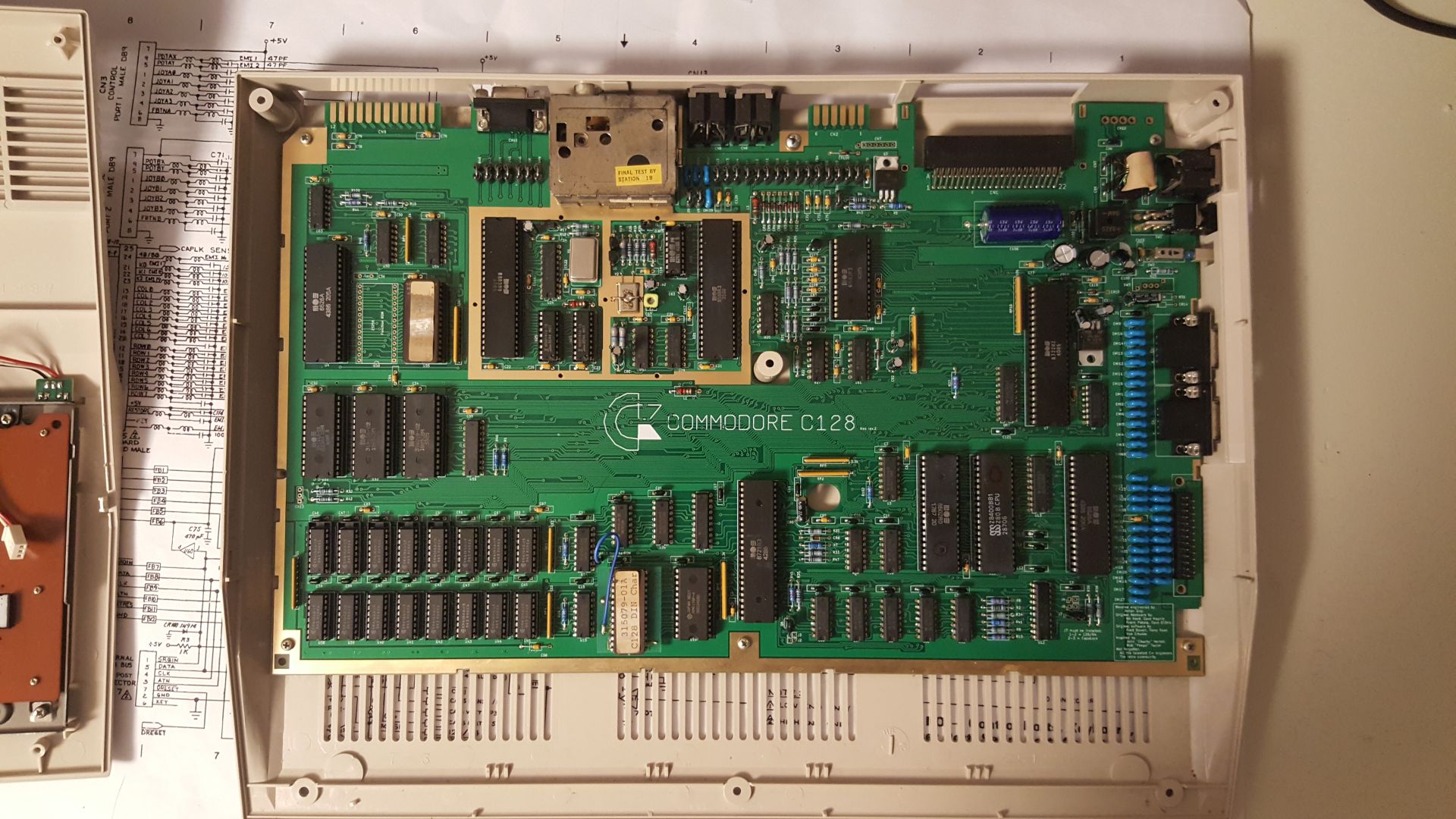
Quite a few improvements since rev.1, not the least of which being mounting holes. This one also shows off some of the small changes I’ve made compared to the original. One example of that is the international character ROM I have in this system, which on the original board requires soldering some jumper wires.
The original US C128 uses a Commodore mask-ROM for the character ROM which is a MOS 2364 chip. These ROMs contain the fonts used by the C128 of which there are four. Upper and lower case C128 mode plus upper and lower case C64 mode. Which font bank was used is then controlled by a signal from the MMU chip telling is the computer is on 128 or 64 mode.
On the international models, the local Commodore branches would replace these ROMs with EPROMs containing the local
characters for the country the machine was sold in. In order to do so and still maintain compatibility for some of more
picky of softwares, they kept the C64 fonts which was duplicated and one set was then changed to the country specific one.
In order to select between US and local fonts, the font bank is now selected using the Caps lock key on the keyboard.
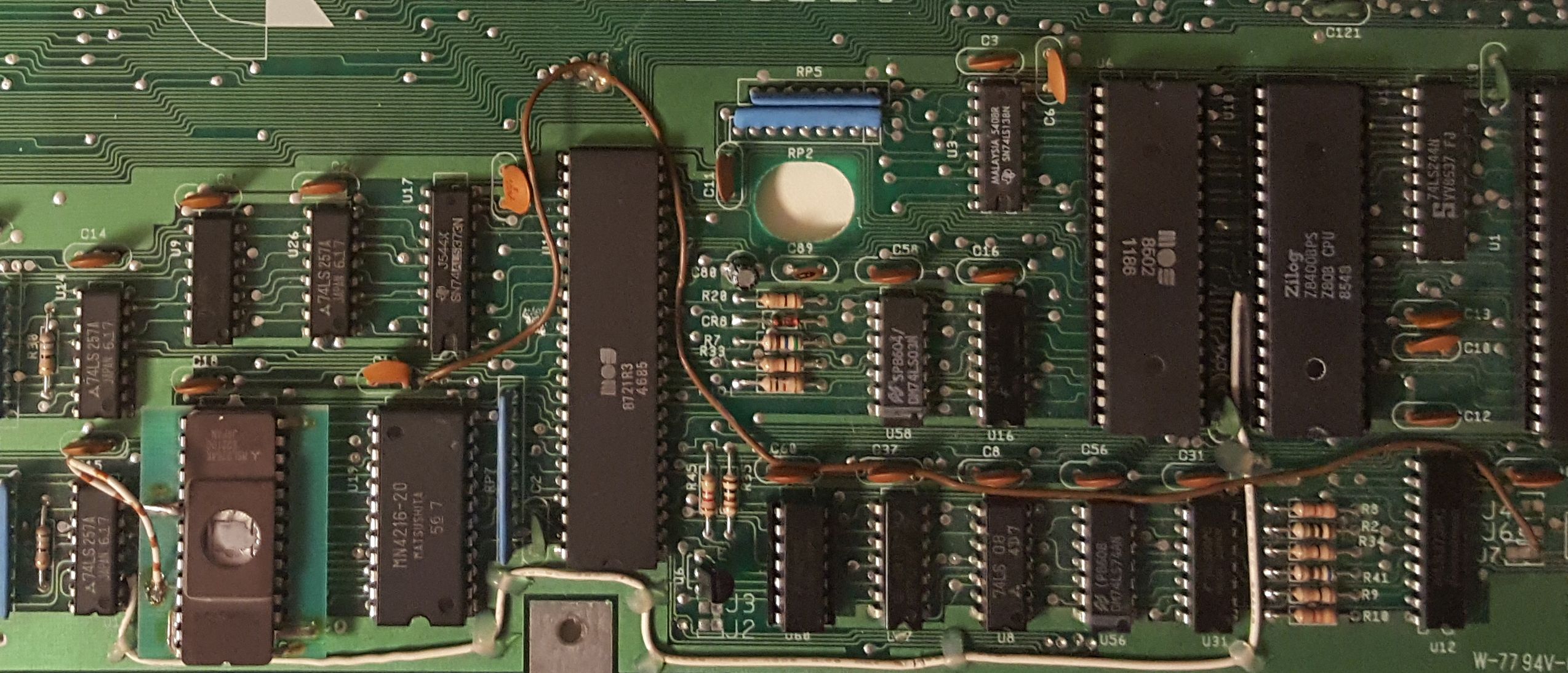
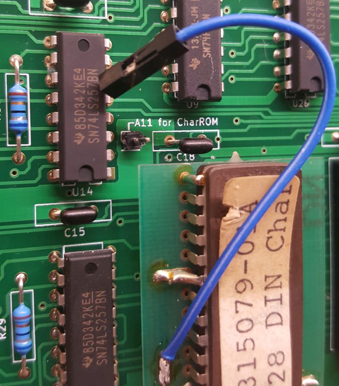
Since the pin-out of the 2364 and the EPROM is not the same, the EPROMs were installed on small adapter boards which can be
seen in the picture above. This adapter requires a wire to be soldered to the A11 signal on the motherboard to work, which
is the white/brown wire on the left side.
In order to make the change from the 64/128-signal to the Caps lock key, a trace was cut and a wire was installed from J7
to the font bank signal, which is the brown wire on the picture.
J7 was originally intended to be a jumper to do this without any patching of the PCB required, but reasons unknown to me it is not functional on the PCB. It’s shown as intended in the schematic but not wired as such on the PCB.
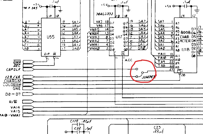
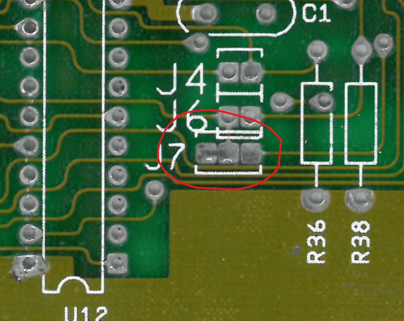
As can be seen on the PCB, even though J7 is three pads only two are actually connected. On the C128Neo this has been implemented as intended in the schematic and changed to a normal jumper layout with pins.
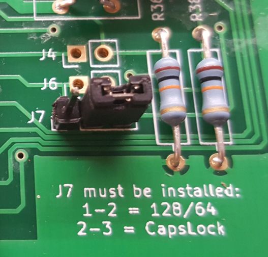
This means there is no longer any need to cut traces and install jumper wires even when the adapter board is used.
Speaking of the adapter board, soldering and de-soldering a wire every time you want to remove the character ROM was getting
tedious so I also made room for a pin header for the A11 signal.
These changes should make for a more convenient daily life with the machine, I hope.