Fixes: R102
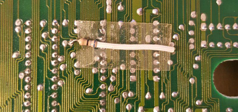
So, I figured I would make a small series of posts on the various little fixes that has been implemented on the C128 Neo boards. First up is this little fellow that is manually soldered to the underside of the PCB close to the 8502 CPU.
Since there are no markings I ended up following traces around to figure out what it is for.
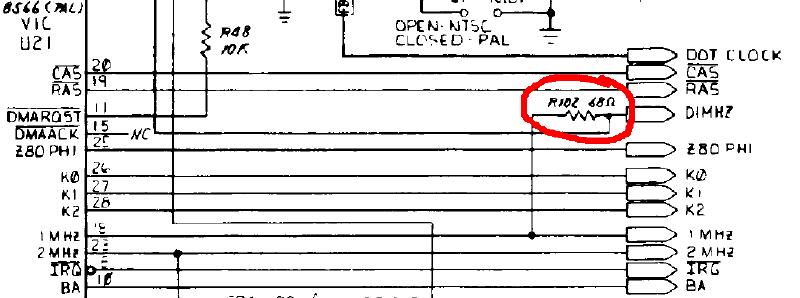
In the commodore schematic it is marked as R102 and sits between the 1MHZ and D1MHZ lines.
As to why it exist, I’m not entirely sure. I know it was introduced in rev 7 of the schematic, on rev 6 there is no D1MHZ and all points that had this signal is fed straight from 1MHZ off the VIC. I suspect there were some corner cases where things misbehaved, external hardware doing silly things or maybe just something related to meeting RF emission regulations.
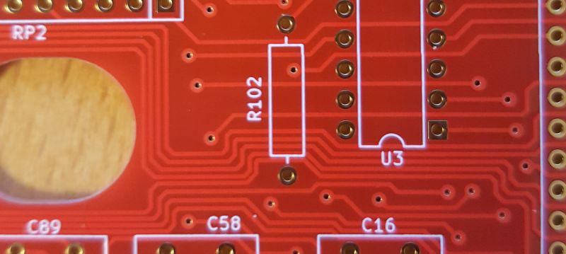
In any case on the C128 Neo R102 was given an actual footprint. I had to do some minor re-arraging of the traces around it but it ended up fitting it pretty nicely.


